Greg Yeric, Arm Fellow and DAC 2020 keynoter, cautions about the manufacturing changes coming for the EDA and semiconductor industries.
August 4, 2020

One of the hot topics at this year’s virtual Design Automation Conference (DAC) was the coming impact on manufacturing resulting from the end of Moore’s Law. Greg Yeric, a fellow in Arm’s Research Group, spoke about this challenge in his keynote address.
His focus was on the huge obstacles faced by chip design and especially manufacturing between now and 2030. He warned that the industry’s underlying technology faces some “extreme” challenges. Basically, the existing Design for Manufacturing paradigm will need to adapt quickly to allow some radically different opportunities to carry the electronic design automation (EDA) and semiconductor industries to 2030 and beyond.
|
Transistors that got us to the Moon. (Image Source: DAC 2020 Arm Greg Yeric Keynote - Moon) |
Yeric began by highlighting the incredible progress that been made over the course of the last 55 years, from the six transistor chips that got us to the moon to the 68,000 transistor chips that ushered in the dawn of the pc connected internet. Today, 30 billion transistors used in the AWS Graviton2 processor that put us firmly in place of a new data economy.
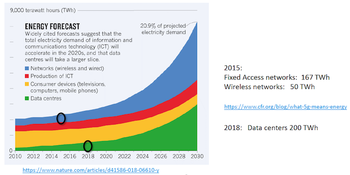
He cautioned that with this amazing progress comes global responsibility. The systems that the EDA and semi community have enabled are using an increasingly large slice of the world's energy output. Numerous new headlines have attested to how Facebook and Google data centers, as well as Bitcoin mining, continue to gobble up most of the world’s electricity. This is particularly concerning from a sustainability perspective as the chip and electronics industry continues to grow.
Just one example of this continued growth comes from the much-anticipated roll-out and proliferation of 5G technology, which will shift the data paradigm from person-to-machine connectivity to machine-to-machine in just a few years. According to Yeric, that trend is shown in energy forecasts as inflection points right around the time from a consumer device-dominated perspective to one that's taken-over by networks and data centers.
|
Data poised to dominate. (Image Source: DAC 2020 Arm Greg Yeric Keynote - Nature) |
The sustainability issue is partially being addressed by the continuing push for lower-power chips and systems – mainly to extend the battery life of mobile devices. But another driver is cost. As Yeric pointed out, engineers can continue to design and manufacture the lowest power, fastest machines but it does little good if no one can afford them. And that’s the problem. At lower chip geometries, the purchase price of tools required to stay relatively on track with Moore’s Law are becoming cost prohibitive. For example, the current EUV chip wafer manufacturing system costs over $100 million US and requires three Boeing737s to transport. The newer High-NA EUV will cost $255 million per platform and require a laser more powerful by energy than the test system that the US navy is using to shoot down missiles. This is not an energy or cost sustainable trend.
Another driver for the need for increased sustainability comes from machine learning tools used in the ever-growing data economy. But as Yeric cautioned, machine learning requires a trade off between programming complexity for training. Unfortunately, with today’s semiconductor hardware, that training uses an enormous amount of energy. Yeric cited the common example of the AlphaGo Zero project in which 25 million dollars in hardware was required for the 216-megawatt hours to train the system. If the current trend is extrapolated out, then a training budget of 280 Yata flop days will be needed in the 2030 time frame. Yeric concluded that machine learning must become more efficient to provide a sustainable path to the future.
What manufacturing options might help overcome the challenges of our current lithography-based semiconductor systems? One might be molecular self-assembly, which is already being used in healthcare to cure cancer in mice using DNA origami.
Further, Yeric explained that our current semiconductor approach is very limited by the two-dimensional nature of putting down contacts and wires to transistors. That was another reason why something like molecular self-assembly holds promise for the future – even if it is a speculative technology.
New materials and new physics – like transmonics, skymonics, photonics and others - will also be needed to produce electronics in a sustainable way by 2030. But these new approaches look so different from the current semiconductor CMOS technology that they are not going to be useful to benchmark or extrapolate from an existing design flow, cautioned Yeric. This will make it challenging for innovative companies to invest in the new needed processes – as they will need not only a new technology but new tools and manufacturing techniques.
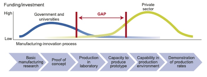
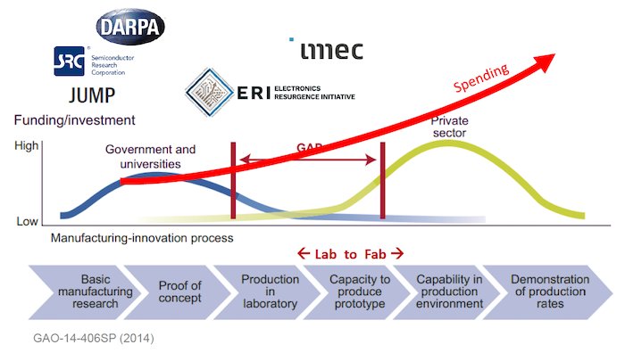
These issues with chip design and manufacturing is part of a broader topic that's often referred to as the lab-to-fab gap. According to a US GAO report on nanomanufacturing emergence: “U.S. funding/investment gaps may undermine U.S. innovators' attempts to transition nanotechnology from R&D to full-scale manufacturing.”
Yeric noted that certain public sector companies are working on interesting technologies to fill some of the gap area, such as ERI and Imec. Still, the scale and precision required to move down the leading-edge CMOS nodes would significantly expand this gap. Further, any new fundamentally different technology will really have to prove itself to the private sector. Together, these realities will actually increase the gap.
|
Lab-to-Fab. (Image Source: DAC 2020 Arm Greg Yeric Keynote - GAO) |
But there is some good news. There is renewed interest by the US government to spend money in the semiconductor manufacturing area. While several bills in Congress are earmarked towards funding of conventional manufacturing facilities – like the proposed fab in Arizona – Yeric believes that some of the wording of the bills would enable significant resources to be applied towards addressing the lab-to-fab gap. It might even be a good idea to have a national nanoelectronics lab created in the US.
In summary, Yeric explained why the time period between now and 2030 would see the emergence of several new and viable – call them post-Moore’s Law – beyond CMOS options for manufacturing of electronics. But this would only happen with the combined efforts of the EDA and semiconductor manufacturing communities (and the government) to bridge the lab-to-fab gap.
While Yeric’s original presentation was part of the DAC 2020 event, his talk has been reposted in its entirety on the following Youtube site:
John Blyler is a Design News senior editor, covering the electronics and advanced manufacturing spaces. With a BS in Engineering Physics and an MS in Electrical Engineering, he has years of hardware-software-network systems experience as an editor and engineer within the advanced manufacturing, IoT and semiconductor industries. John has co-authored books related to system engineering and electronics for IEEE, Wiley, and Elsevier.
About the Author(s)
You May Also Like


